New 388 problem

I did answer it but in a roundabout way...the coarse instructions I gave for what we will do with those clip leads guided you to put everything back together after having the clip lead in place. So...the ideal would be to disassemble whatever necessary to get a lead hooked to a 'G' leg of either Q101 or Q102, and then connect everything back up and conduct the test.

So here is what you will do when you can get to it:

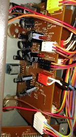
1. Connect a flying lead to the 'G' leg of either Q101 or Q102
2. Ensure all L-R assign switches are in the up/unlatched position
3. Power on the 388 and, with the + probe of your multimeter connected to the flying lead, and the - probe touching pin 8 of connector P102 on the BUSS B PCB (A-OK to probe the related solder joint on the M BUSS PCB), measure for DC volts
4. Latch any L-R assign switch
5. Measure for DC volts as in step 3
6. Report your measurements

I don't know exactly what voltages you should see...I'm not even sure of what state should result in positive voltage. What I DO know is Q101 and Q102 are like little gates...with voltage at a certain state at their 'G' terminals, the connectivity between their 'S' and 'D' terminals is pinched off. This is what should be happening when any L-R assign switch is latched. What I *think* is happening is the IC array U101, U102 and U104 is not functioning properly and Q101 and Q102 are always seeing the same voltage state at their 'G' terminals regardless of the state of the L-R assign switches. So rather than looking for a specific voltage in steps 3 and 5 above, we are looking to see if there is any significant *change* when any L-R switch is latched. We have tested to make sure power is getting TO U101, U102 and U104...we have tested to make sure audio is getting TO Q101 and Q102. So now we are testing to see if anything is happening at those control terminals 'G' of Q101 and Q102 when an L-R assign switch is latched. If there is little or no change between the voltage measurements at steps 3 and 5 above, that further reinforces something is wrong with the U101, U102 and U104 array, and because I have dealt with MC14069 failures on more than one occasion on a 388 in the past, my advice would be to go forward and shotgun U104.

Oh yeah, you're right, you did answer that. My bad!

Ok sounds like a plan. I'll try to get to it tonight. Thanks!
 
Ok ... a slight detour here. I was getting ready to take those measurements when I realized that I had already removed the old MC14069 chip. So I need to wait until the new one gets here so I can install it.

However, I was looking at the PCB and noticed some unpleasant things. See the attached picture.

1. I lifted one pad entirely when removing the U104 chip and lifted most of another. :( The one on top, which is pin 6 (pin 1 is the lower left terminal in this picture), shouldn't be an issue since it's not connected to anything, correct? For the one below it ... pin 5 ... I should just be able to run a jumper wire over to pin 11, correct (see blue line)?
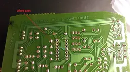
2. There are two scrapes in the traces (circled in yellow). I don't know for sure if I did this while removing the chip. It's possible, because it did not exactly go gentle into that good night, but I didn't notice them right away if I did it. I know I did manage to scrape a bit right underneath the chip, but it seems as though that trace should still be functional, yes?

However, if I did not make these scratches, could that possibly be the culprit? Those traces are connected to Q103 and Q104. They connect all the way over at the other end of the board at the ribbon connectors P102 or P101.

I guess I'll need to run jumper wire from those Q103 and Q104 terminals to the their connections at P101 or P102, yes?

3. Just curious ... Regarding pin 11 (and pin 5, for that matter), I can clearly see that it's physically connected, via traces, to some diodes and capacitors --- looks like D102 and C104 and D103 and C105. But when I look at the schematic (page 4-6), I can't find reference to pin 5 or pin 11 for the U104 chip. All I see are pins 1, 3, 4, 12, 13, and 14. What am I missing here?
 

Attachments

  • Buss B PCB close up.jpg
    Buss B PCB close up.jpg
    370.8 KB · Views: 8
A conversation from last night

Brad: "Whatcha reading?"
Wife: " Some kind of action thriller..... What are you reading?"
Brad: "A mystery"
Wife: "Whats it called?"
Brad: "New 388 Problem...."
Wife:".........it's times like these that I can't believe I married a geek......."

Keep it up boyz...... I need to see how this story ends!!!! :)

Ha! :)

I'm ready for it to end too! I'd like to button this guy up and get the tape a rollin' again.
 
1. Yes looks like don't worry about pin 6. For pin 5 if it was me I would just use a very small flat blade screwdriver to remove some of the green varnish from the board right by the damaged solder land for pin 5, tin it, and then when installing the new part just bend pin 5 over to the board and solder it in. You could also do a jumper, but my suggestion involves less potential for additional damage. These phenolic boards are difficult to work on. I use a small pencil iron that's still pretty hot, but with the small tip I can get in there and work pretty quick. That's the key.

2. Measure for resistance between two points that border the exposed traces. If you get a dead short the traces aren't damaged...just some of the varnish got scraped off. No big deal. But measure/test before you go start an unnecessary repair. If the traces are damaged, take that flat blade screwdriver and expose more trace, tin the exposed trace, then clip a leg off of a new resistor or capacitor to use as a bridge over both sides of the damaged trace and solder it in. I suspect your traces are fine.

3. What you are dealing with is an out-of-date or erroneous schematic. I used to know of only two errors in the 388 manual before this thread. You've enlightened me.
 
Ok, I checked those two scrapes in the traces and got 0 resistance. I assume this means a dead short, correct?

I got the new MC14069 installed. I checked resistance from pin 5 to pin 11 and got 0, so I'm assuming pin 5 is connected well. Got everything connected again.

I was able to measure from pin G on Q102 with the flying lead (I don't even know if I could get it on Q101), and here's what I got:

All L/R buttons up (unlatched): 348 mV
Ch. 1 L/R button down (latched): -7.6V
 
Um, that would be a big 10-4! :) I am getting monitor buss signal now!

However, I think you were right way back when you said I might have two issues, because:

Although the monitor buss signal is working loud and clear in the phones, it's very weak coming out of the MON OUT jacks. It's the same issue as what was described back in post #39.

But, damn we're close now! :)

Those damn MC14069 chips!
 
Progress!!!

Fantastic!

Okay. I'll dig back into the schematics when I can for next steps with the MONITOR OUT jacks...it is a more simple issue (i.e. not logic related) for sure because of where the signal branches between the phones and the jacks.

Yay! :guitar:
 
Progress!!!

Fantastic!

Okay. I'll dig back into the schematics when I can for next steps with the MONITOR OUT jacks...it is a more simple issue (i.e. not logic related) for sure because of where the signal branches between the phones and the jacks.

Yay! :guitar:

Yes, awesome! You seriously rock Cory! :)
 
So we're now going to shift our focus to the PHONE AMP PCB. This is a board that houses the headphone amp and MONITOR OUT amp. Since both of those amp sections are sharing the same signal source, and one works and the other doesn't, it's a pretty safe assumption there is either something wrong with the monitor amp, or something wrong with the connections between the output of the amplifier and the jacks right? That make sense?

The PHONE AMP PCB I *believe* is mounted to the underside of the transport control panel. Have a look under there. I can't remember if it is right "there" when you tip the machine up and remove the bottom cover, or if it is underneath another board...you'll have to tell me what you see there. If possible, if you can get to the back side of the MONITOR OUT jacks, find the wires that bring signal to those jacks and follow them back to where they plug in...wherever they plug in, that's the PHONE AMP PCB...should be a red 3 pin connector that connects to P103 on the PHONE AMP PCB.

BTW I'm looking at all this on page 4-18 of the service manual.

First thing I want you to do is exercise that connection and see if there is any improvement in the output level of the MONITOR OUT jacks.

Let's just start there...locate the next board we're going to be working on, locate where the MONITOR OUT jacks connect to that board, and make sure we have a good connection there.

Because your problem is across both channels, I suspect the solution isn't as easy as exercising J103-P103, but at least we'll get oriented to what's where.

If you can put up a picture of what the area with the PHONE AMP PCB looks like, that would help me help you. I'm sure I have one somewhere, but I don't want to go hunting.
 
Ok, here are some pictures of the PHONE AMP PCB.

I removed the P103, sprayed some Deoxit, and plugged it in several times.

Interesting turn of events. There's no change in the volume level out of the MON jacks, but now the right side of the MON buss sounds crunchy, both in the phones and out the MON OUT jacks. I tried different cables and input channels on the 388, made sure I wasn't distorting the input (because it kind of sounds like that), and the problem always stays with the right side of the MON buss.

I have signal routed to CH 1 and 2 inputs on the 388, both are assigned to 1/2, and the 1 and 2 REC buttons are pushed. I can pan either Monitor knob (1 or 2) to the left, and the signal is clean. But when I start panning either to the right, at around 10:00 or so, it starts to crunch up on the right side.

When I listen to the L/R mix in the phones, it sounds perfect, as it does through the speakers too. So I'm fairly certain it's still limited to the monitor buss.

Literally the only thing I've done to it since this afternoon was what I mentioned above. After trying it out this evening and having this new issue, I went ahead and replugged all the connectors on the PHONE AMP PCB just to see if it did anything, and there was no change.

I'm 85% sure that the playback was clear on both sides of the monitor buss this afternoon, but I can't be 100% sure. I just realized that when I checked it earlier today, I was listening to a very distorted, crunchy Tom Petty song ("Change the Locks"), so it is possible that it was like this then, and I just didn't notice it because I was so happy to hear strong signal through the monitor buss. I didn't listen to it through the phones for very long before I started trying the MON OUT jacks. I thought I listened to another song through the phones, though, but I'm not positive.

Bizarre? Anyway, I'm hoping this is all connected somehow. It's a bit of a bummer, but I'm still very encouraged, because crunchy sound through one side of the monitor buss and clear on the other is still a lot better than no sound at all!
 

Attachments

  • close.jpg
    close.jpg
    177.5 KB · Views: 2
  • closer.jpg
    closer.jpg
    174.1 KB · Views: 3
  • Overview.jpg
    Overview.jpg
    177.6 KB · Views: 2
Well ... what the hell. The MON buss seems to working fine now in both channels on the phones.

The only thing that happened since my last post was that I noticed I had never removed the flying lead from Q102. So I pulled out the M BUSS card and pulled a few other connectors I needed in order to reach the lead. I put everything back together and decided to give it one more shot, and I was getting absolutely nothing in the phones at all. Not even through the main mix.

At that point, I was like ... "Ok, this must be something I did." So I retraced my steps and found that I had inadvertently pulled out a small three-pin connector on the BUSS B PCB while I was getting to the flying lead. I plugged that back in, and now I'm getting clear sound in both sides of the phones with the monitor buss again.

I don't know exactly what happened. But ... I guess we'll see if it holds.

So ... for the time being, you can ignore that "turn of events" part of my previous message. We seem to be back where we were in post #131. :)
 
Is it possible to unmount the PHONE AMP PCB and still have it all hooked up (so you can have the system powered and be able to probe different points on the component and/or solder side)? This will likely be necessary in order to locate the culprit.

I *suspect* the monitor output buffer amp U103 is shot. The present symptoms you describe sound to me like a bad opamp, and this is reinforced by the change in symptoms...I think it was dying...the diminished output was its swansong, and when you cleaned the connections it could have been enough change on the output impedance or something to tip it over the edge.

I could be completely wrong.. That's just what my gut is saying.

So, like a Choose Your Own Adventure book (does anybody else remember those?...dating myself there but I loved reading those as a kid...), you get to choose trace it out and affirm the culprit, or shotgun U103, or maybe something in between.

While you're thinking about that, without playing audio through the monitor buss, is there any random or excessive noise coming out either channel of the MONITOR OUT jacks? If so, does the monitor level control effect the noise level, and does the noise sound the same in both channels?
 
Do this...I want to know where the monitor level control needs to be set so the input level to the monitor amp equals the output level.

1. Route a 1kHz tone to the monitor buss
2. Find the black 3 pin connector P101 on the PHONE AMP PCB...that's the input to the board
3. Set your meter to AC volts and measure between pins 1 and 2 of P101; hopefully you've got a decent level there like around 300mV
4. Now that you have a given level at the input (the one you just measured in step #3), measure for AC volts between pins 1 and 2 of the red connector P103 (the output of the board)
5. Adjust the monitor level control to achieve the same level on P103 as on P101
6. What position is the monitor level control in? 3:00? 4:00? 5:00?
 
Ok, I'll get to this hopefully maybe tonight or tomorrow. Thanks!

These are the kind of homework assignments I don't mind. :)

And, yes, those books were totally awesome! I had 7 or 8 of them I think. Good times.
 
Last edited:
Ok, I think I should be able to get the PHONE AMP PCB accessible, but I haven't yet. It looks as though the only thing holding the it in place are the three pots (pitch control, vari/fix/ext, and phones/monitor). But when I tried to remove the knob for the pitch control. It didn't want to come off. Do you remember if there was any trick to getting those three knobs off?

It was kind of odd. I got some pliers and tugged on it, and it started to come up a good way as if it were coming off the shaft, but then it stopped again and started to give a lot of resistance. At that point, I backed off because I didn't want to do any damage. So I figured I'd ask you if you remember anything special about those before I tried again.

Regarding the 1kHz tone test:
You didn't mention how hot you wanted the signal, so I set it at 0dB on CH 1, had the CH 1 MON gain knob fully up and panned fully left.

With that, I got a reading on P101, pins 1 and 2, of 187 mV.

With the MON/PHONES knob turned up to max, I got a reading of about 175mV on P103, pins 1 and 2.
 
Back
Top