

sweetbeats
Reel deep thoughts...
So, random post. But maybe not so random.
The M-__ has mostly been just sitting under a custom LeCover for since my last post, but recently I’ve been prepping to capture a series of videos detailing the features and functions of the M-__. This is something I’ve been wanting to do for a long, long time…a video operations manual of sorts. I’ve shared that previously in this long forum topic. But anyway, because I’d like to finally capture those videos I’ve been taking the time to *finally* tease out details of the M-__’s functions and signal flow…I know it’s been, like, 18 years, but life has been crazy, so forgive me. I’ve never fully gone through nailing down ALL of the details of the functions and signal flow aspects of the M-__.
What I mean by that is detail stuff I can’t remember because I don’t use it enough, like the five different SOLO buss sources on each input/output module…where does each specifically tap the signal chain? The MONI TO STEREO switch that sums the monitor buss source on each module to the main buss…is it pre or post channel fader? The CHANNEL MUTE kill switch…what all does it actually mute? There are a total of 19 output channels from each input/output module…I knew off the top of my head the CHANNEL MUTE switch did NOT mute the DIRECT OUT jack. What else? Anything? Now I know. I have a couple other things I want to verify yet, but I’m nearly done going through the whole console with a fine-tooth functionality comb.
In the process, however, I became sidelined with finally clearing up some annoying issues…the signal flow to the STEREO buss has been problematic…both to the audio output as well as to the meters…intermittent…really annoying. And there has also been an annoying problem with the headphone output related to higher than normal noise level and DC popping in the headphones when any of the monitor buss global REMOTE source switches are pressed on the Control Module, which is what Tascam named the module that contains the master fader, oscillator, talkback functions and studio and control room functions as well as the master monitor and “remote” control functions. BUT I’m happy to say I’ve tackled those issues…some reflowing of solder joints as well as reinforcing the wire management took care of the intermittent STEREO buss signal flow and meter monitoring. I’m also finding it’s been enough years now it’s needing some maintenance on the edge connectors that interface the modules to the mother board, so checking the contacts in the sockets on the motherboard as well as a little gentle polishing of the contacts on the module edge connectors and then treating with DeoxIT D100…exercising, etc. It wasn’t bad, but it was time to do something and I want to take that variable out of the mix if I am troubleshooting a problem. Anyway, STEREO buss problem fixed. The headphone issue…I used to have a quote at the bottom of all my posts: “Never underestimate your capacity to be a complete ignoramous”…something like that. Well, I’ve done it again. Many years ago I cleaned up a VERY kludgey abomination of a circuit block on the “Phono Amp PCB” assembly in the Control Module. That’s the right-most PCB assembly of the four main boards in the module. I can’t remember what the function of that circuit block is at the moment, but I detailed it in this thread years ago…stacked opamps, one in the board and the other upside-on top of the first, just hanging in free space held only in place by the point-to-point wiring and components soldered to its pins…no judgement…it is a prototype device after all, and sometimes these kinds of things are even incorporated into production models by any manufacturer. But it was messy and I wanted better access to both opamps, so I modified things, moved one opamp into a vacant DIP8 site on the board, incorporated some jumper wires, etc. In that process I noticed the signal ground pins of the headphone level pot were referenced to signal ground via the shield of one of the output wires. So let me explain the level pot and the source switches for the headphone amp are on the right-most of the four PCBs, but the amp itself is on the left-most of the four PCBs. So there are wires from the two output pins of the level pot on the right-most PCB that go the amplifier input solder joints on the left-most board. The shields of those wires are also terminated on the PCB with headphone amp circuit block. But they also terminated the shield of one of those wires on the right-most board on a hand-added solder pad in order to connect the signal grounds of the level pot to signal ground on the PCB with the amp. Maybe that’s fine. But I wanted both channels’ shields to float at the pot so they could both properly shunt any induced noise interference to ground on the board with the amp…float at the source, shunt at the load. So I did that. And then found the closest place on the PCB with the level pot to strap the signal ground to the appropriate ground path…the headphone amp is powered by a +6VDC power supply, which also powers the meter lamps and LED indicators, so the ground reference for that supply is on almost every PCB in the console. So it made sense to me to just jumper the headphone level pot signal grounds to the closest spot where that ground was available on the same PCB as the level pot. Nope. What I didn’t understand at the time or think through at the time is the potential for DC offset by doing what I did. The original reference to ground through the shield of the one signal conductor strapped the signal ground of the level pot close to the amplifier circuit block ground path, as well as very close to where the PCB with the amp references system ground at the motherboard…and more importantly the +6V rail reaches the LM386 opamps in the headphone amp directly…no dropping resistor. However the +6V rail goes through a series dropping resistor on the PCB with the level pot. So that enabled some amount of DC offset in the power rail for the headphone amp between the pot and the amp (enabling the *pop* when I would latch any of the monitor buss global REMOTE source switches that are on the same PCB as the level pot, and the switches also power an LED indicator when latched), and beyond that actually increased the risk of noise interference in the headphone amp circuit…and in fact I think raised the noise floor of the headphone amp. I think the reason I didn’t notice after I did those mods years ago is because I wasn’t really focusing on the headphone amp after the mods (more focused on the modified amplifier circuit), and then probably didn’t do anything operationally with the console after that…I think I moved shortly thereafter and then the console was in storage for awhile. By the time I noticed the new problems I bet I didn’t associate them with the mods I’d done because substantial time had passed. Anyway, ground issue fixed…I ran a separate connectorized ground wire from the level pot signal ground pins to the left-most PCB on an available solder pad close to the headphone amp circuit block…no more pop, noise floor better, and proper attenuation. Fixed!
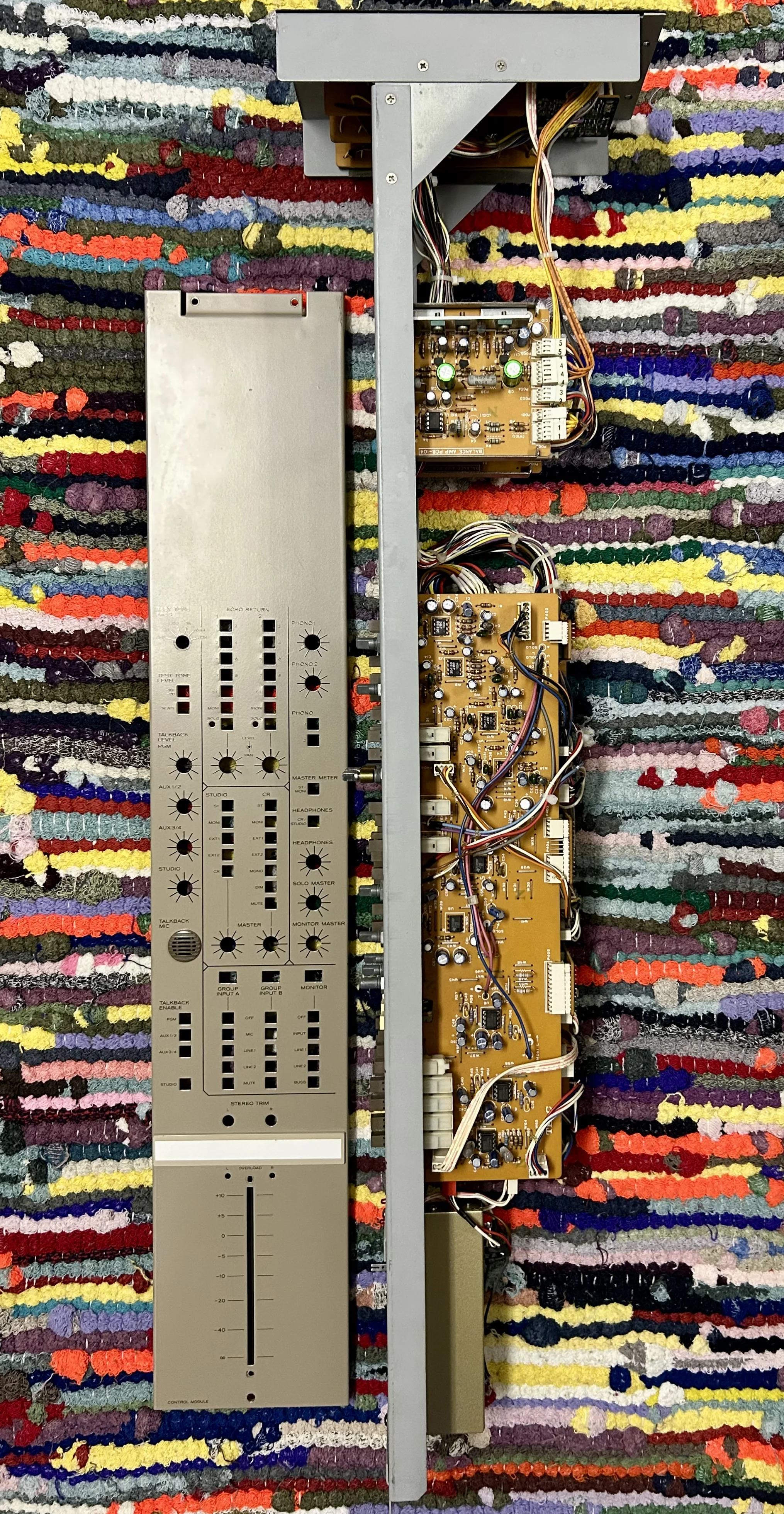
And here is the Control Module ready for final reassembly and reinstallation in the console frame, so I can tease out my last couple question regarding functionality…
Next step is to write out all the details of the control functions on pages I’ve printed with sections of each module…number each and document narrative like in an operations manual…and then capture a video series covering all of this and get it up on YouTube.
The M-__ has mostly been just sitting under a custom LeCover for since my last post, but recently I’ve been prepping to capture a series of videos detailing the features and functions of the M-__. This is something I’ve been wanting to do for a long, long time…a video operations manual of sorts. I’ve shared that previously in this long forum topic. But anyway, because I’d like to finally capture those videos I’ve been taking the time to *finally* tease out details of the M-__’s functions and signal flow…I know it’s been, like, 18 years, but life has been crazy, so forgive me. I’ve never fully gone through nailing down ALL of the details of the functions and signal flow aspects of the M-__.
What I mean by that is detail stuff I can’t remember because I don’t use it enough, like the five different SOLO buss sources on each input/output module…where does each specifically tap the signal chain? The MONI TO STEREO switch that sums the monitor buss source on each module to the main buss…is it pre or post channel fader? The CHANNEL MUTE kill switch…what all does it actually mute? There are a total of 19 output channels from each input/output module…I knew off the top of my head the CHANNEL MUTE switch did NOT mute the DIRECT OUT jack. What else? Anything? Now I know. I have a couple other things I want to verify yet, but I’m nearly done going through the whole console with a fine-tooth functionality comb.
In the process, however, I became sidelined with finally clearing up some annoying issues…the signal flow to the STEREO buss has been problematic…both to the audio output as well as to the meters…intermittent…really annoying. And there has also been an annoying problem with the headphone output related to higher than normal noise level and DC popping in the headphones when any of the monitor buss global REMOTE source switches are pressed on the Control Module, which is what Tascam named the module that contains the master fader, oscillator, talkback functions and studio and control room functions as well as the master monitor and “remote” control functions. BUT I’m happy to say I’ve tackled those issues…some reflowing of solder joints as well as reinforcing the wire management took care of the intermittent STEREO buss signal flow and meter monitoring. I’m also finding it’s been enough years now it’s needing some maintenance on the edge connectors that interface the modules to the mother board, so checking the contacts in the sockets on the motherboard as well as a little gentle polishing of the contacts on the module edge connectors and then treating with DeoxIT D100…exercising, etc. It wasn’t bad, but it was time to do something and I want to take that variable out of the mix if I am troubleshooting a problem. Anyway, STEREO buss problem fixed. The headphone issue…I used to have a quote at the bottom of all my posts: “Never underestimate your capacity to be a complete ignoramous”…something like that. Well, I’ve done it again. Many years ago I cleaned up a VERY kludgey abomination of a circuit block on the “Phono Amp PCB” assembly in the Control Module. That’s the right-most PCB assembly of the four main boards in the module. I can’t remember what the function of that circuit block is at the moment, but I detailed it in this thread years ago…stacked opamps, one in the board and the other upside-on top of the first, just hanging in free space held only in place by the point-to-point wiring and components soldered to its pins…no judgement…it is a prototype device after all, and sometimes these kinds of things are even incorporated into production models by any manufacturer. But it was messy and I wanted better access to both opamps, so I modified things, moved one opamp into a vacant DIP8 site on the board, incorporated some jumper wires, etc. In that process I noticed the signal ground pins of the headphone level pot were referenced to signal ground via the shield of one of the output wires. So let me explain the level pot and the source switches for the headphone amp are on the right-most of the four PCBs, but the amp itself is on the left-most of the four PCBs. So there are wires from the two output pins of the level pot on the right-most PCB that go the amplifier input solder joints on the left-most board. The shields of those wires are also terminated on the PCB with headphone amp circuit block. But they also terminated the shield of one of those wires on the right-most board on a hand-added solder pad in order to connect the signal grounds of the level pot to signal ground on the PCB with the amp. Maybe that’s fine. But I wanted both channels’ shields to float at the pot so they could both properly shunt any induced noise interference to ground on the board with the amp…float at the source, shunt at the load. So I did that. And then found the closest place on the PCB with the level pot to strap the signal ground to the appropriate ground path…the headphone amp is powered by a +6VDC power supply, which also powers the meter lamps and LED indicators, so the ground reference for that supply is on almost every PCB in the console. So it made sense to me to just jumper the headphone level pot signal grounds to the closest spot where that ground was available on the same PCB as the level pot. Nope. What I didn’t understand at the time or think through at the time is the potential for DC offset by doing what I did. The original reference to ground through the shield of the one signal conductor strapped the signal ground of the level pot close to the amplifier circuit block ground path, as well as very close to where the PCB with the amp references system ground at the motherboard…and more importantly the +6V rail reaches the LM386 opamps in the headphone amp directly…no dropping resistor. However the +6V rail goes through a series dropping resistor on the PCB with the level pot. So that enabled some amount of DC offset in the power rail for the headphone amp between the pot and the amp (enabling the *pop* when I would latch any of the monitor buss global REMOTE source switches that are on the same PCB as the level pot, and the switches also power an LED indicator when latched), and beyond that actually increased the risk of noise interference in the headphone amp circuit…and in fact I think raised the noise floor of the headphone amp. I think the reason I didn’t notice after I did those mods years ago is because I wasn’t really focusing on the headphone amp after the mods (more focused on the modified amplifier circuit), and then probably didn’t do anything operationally with the console after that…I think I moved shortly thereafter and then the console was in storage for awhile. By the time I noticed the new problems I bet I didn’t associate them with the mods I’d done because substantial time had passed. Anyway, ground issue fixed…I ran a separate connectorized ground wire from the level pot signal ground pins to the left-most PCB on an available solder pad close to the headphone amp circuit block…no more pop, noise floor better, and proper attenuation. Fixed!
And here is the Control Module ready for final reassembly and reinstallation in the console frame, so I can tease out my last couple question regarding functionality…
Next step is to write out all the details of the control functions on pages I’ve printed with sections of each module…number each and document narrative like in an operations manual…and then capture a video series covering all of this and get it up on YouTube.


