Do It Yourself Neve 1073

Neve1073lover

Inset French Saying Here
Hello all.
Just completed a Linear-Recording based Neve 1073 clone.

Propose to document the issues, design errors and any hints I can think of in this thread.

I have also built several valve amps (Weber JTM45 and 2 x AX84) and two cabinets. Photos are in my photobucket account 'Ozzygazza' (cannot post URLs yet)

Happy to answer any questions and will add to this thread over time.
Garry
 
There are a bunch of us who would be interested to see this (many of us having just bought 1073 "inspired" units in a group buy).

I'm torn as to whether the DIY forum below would be a better place for the thread, though.
 
Yeah, I'm wondering if we should move this to the DIY forum also. I'll leave it here for a day or so to give the OP time to respond.

Hey NeveLover, once you get 5 posts you'll be able to post links. A lot of people will be interested in what you have going on.

Please don't let this become a commercial endeavor, meaning, you can't use the forums to promote a product or service you're trying to sell. But sharing info is what it's all about!! :)

Thanks for posting, look forward to hearing more.

peace.
 
Two AX84s etc.

Yeah, welcome to the forum. I just bought a P1 kit and the parts for a Firefly and am getting after it next week so I will enjoy your building experience. ;)
 
Yeah, I'm wondering if we should move this to the DIY forum also. I'll leave it here for a day or so to give the OP time to respond.

Hey NeveLover, once you get 5 posts you'll be able to post links. A lot of people will be interested in what you have going on.

Please don't let this become a commercial endeavor, meaning, you can't use the forums to promote a product or service you're trying to sell. But sharing info is what it's all about!! :)

Thanks for posting, look forward to hearing more.

peace.
Move to DIY.
Not a commercial anything. Happy to give the designs for the daughterboards and the Front panel away. Just didn't want to waste my efforts.
 
One of these decades I'll get handy with a soldering iron and have a crack at some of this myself. Until then, the DIY forum will remain a mystery to me. Does seem like this idea is particularly "on point" right now though. :p
 
thread_is_worthless-1.jpg
 
My 5th post.

I am uploading all of my pictures to Photobucket so I can get started.
I will probably email any design files to members only for the moment to keep them in the forum. Trying to remember all the problems so I can cover them.
Garry
 
Making the Boards

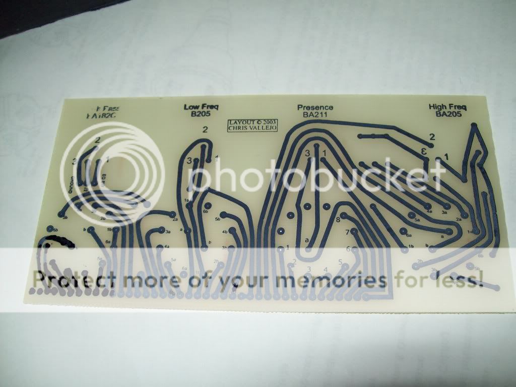
As I said, I used Linear-Recording's 'all in one' design.
It is an accurate copy, other than the power smoothing electrolytic capacitors are 10x what Neve used. Not a problem.

I used 'Press-n-Peel PCB Transfer Film' that costs about $10AUS per A4 sheet.

Cut the PCB with a hacksaw to size.

You print the design using a laser printer with the toner turned to maximum.
Clean the PCB board with steel wool and wash thoroughly. Do not touch the surface afterwards(oils).

You iron the design on with a dry iron set near max. No steam or water.
Put baking paper over the top and iron onto this.

Large boards need more heat than small boards. Takes about 3 minutes. Move the iron around slowly and make sure you spend 60-70% of the time near the edges (they cool quicker and need more heat).

After 3 minutes carefully lift up one edge. If the plastic sheet has totally stuck to the pcb or the design near the edge stops you carefully lifting the plastic, then you are done. If not, lower carefully down and do another minute and retest.

You then quench under a cold tap and carefully lift the plastic off.

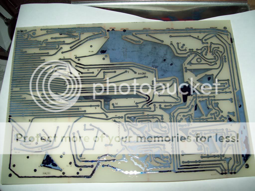
You should now have blue lines:

100_0528.jpg


100_0527.jpg


You use a special pen to touch up the design. This is black in the photo.

You could use photoresist boards, but this is more expensive and I could not get photoresist pcb boards big enough for the Linear-Recording 'all in one'.

Visually check the board for 'shorts' and use a sharp point to scratch between any connections that should not be there.

The best etchant is Ferric Chloride. Put a mix into a flat pan and rock from side to side. Takes about an hour for this large board.

If you think that it is going too slow, pour out the old solution and add new.

Don't add new to old as you are diluting the new...

It is best to leave as is until you are going to start populating the board to stop copper corrosion and soldering problems.

When ready, clean the blue film off using steel wool in a sink of water.

You can try running solder along the tracks, but looks aweful and may cause other problems.

Now check for shorts between every board connection. Use a sharp point to scratch between any. With a multimeter set to 'Ohms' and set to make a sound if there is a 'short', move the points of the probes across the boards where they will connect together. None of these can be connected. THIS IS REALLY YOUR ONLY CHANCE TO FIND THEM!!!!!!

Also go around the board and check copper runs are not connected to any others (unless by a roundabout route - they are actually part of the same run).

Also check that the ends of each copper run are connected (ie there IS a short). Check all branches of the run are connected. You are looking for cracks or discontinuities. Solder over any found.

Try and be systematic and check all of the board. Problems are easier to find now than when you put in components.

Till next time - Garry
 
Last edited:
I was the one who posted the funny pic this thread is worthless without pichers
no need to re post it now that you have posted your pictures Thanks again for the visual aides.
 
I was the one who posted the funny pic this thread is worthless without pichers
no need to re post it now that you have posted your pictures Thanks again for the visual aides.

I think the chap who removed it didn't get the joke, but it looks like it was an innocent mistake - no harm intended.

:)
 
Populating the Switch Board

Start on the smaller board so you can practise your soldering etc. It also allows you to measure up the 2RU rack or whatever you are going to mount it in and drill etc the front panel.

The schematic for a Neve 1073 is all over the Web. Get a copy. You will need it.

Drill the boards. I bought a set of small drills from Dick Smith in Aus.

100_0531.jpg


The switches come in two type: single or double throw.

You use 3xdoubles and 1xsingle (the Presence BA211 switch).

Each switch has a washer that has a prong in it that stops the switch rotating. Set each one to allow for the correct number of positions when you are mounting the board on the front panel.

From R to L it is 3,7,4,4 (plus the Off position). ie there are R-L 4,8,5,5 distinct switch positions. You are looking at the switches from the other side of the pcb.

I bought my switches from Jaycar is Aus and they fitted perfectly.

I bought the capacitors from Jaycar and Mouser in the US. Also bought some parts from Farnell (worldwide). The simple transisters came from Mouser.

I used male pins (from Jaycar) that have the correct spacing for the board connections. I was going to use flat cable, but did not think that the wires were thick enough. Ended up soldering each connection individually with shrink wrap over each connection.

I used Jaycar 13x0.12mm wire for all but power connections and I DO NOT recommend it. It is brittle and breaks too easily at the soldered joint. A real PITA. Try and find a good quality tinned wire about this size.

No electrolytics on this board so no direction problems. The circular switch can only go in one way.

The potentiometers (pots) are above the switches in this design. They were on the end of the switches in the original Neve design. You cannot buy the old design so live with it.

The RH switch is the gain that is normally on the larger board. Put here mainly for looks as far as I can tell. You do not change it. You could omit this and put a trimmer on the larger board if you want.

The pots are connected via wires as they are a different thickness than the circular switches and are mounted separately to the front panel. Use good wire as they will break off easily as you mount the board. Allow for about an inch of wire.

Test the board for shorts etc and also what do you expect to happen at each switch position? Does this happen? Why not? This gets complicated and I cannot help further here.

When you solder, touch the iron point to the pcb pad and the wire. Apply solder to the other side of the wire. When you get the pad covered and a nice curve up the wire (all the way around) you have a good solder joint. It it is dull, redo it.

A good place to break until the next instalment.
 
The 3 Gang 22 Position Switch

I found a 4 gang 24 position military grade (silver contacts) switch on Ebay (Singapore).

If you want to use my front panel, get the same number of positions.

The Neve doco shows how to wire it up (there are two pages).

Note that I used 1/2 watt resistors as you do not need any more and they fit between the pins.

Locate the pin on each gang that is connected to the centre contact that 'sweeps' between the various positions.

This is pin '0'. It is shown as a small 'arrow' on the schematic.

Count anticlockwise from here (looking from the back and mark every 10 pin locations (do NOT count pin 0). You can then keep track of the locations.

Gang 1 is called S2a on the schematic.
Gang 2 is called S2b.
Gang 3 is called S2c.

There is a complication in that there are a number of resistors that are only conected at one end, with individual wires then going away from each resistor.

Given that we have a 4 Gang, you could connect these between the 2 and 3rd gangs and use the 4th gang for what is called 'S2c' on the schematic.

2 wires would then go off from the 3rd gang when they have all been connected properly. If you do this, bend up the 3rd gang's 'sweeper' to disable it.

My son wanted to make a pcb to take these, so I soldered on individual wires and connected them to the pcb.

100_0539.jpg


I can supply this pcb design if you PM me.

Double check all of the values and locations. This switch makes the dB 'steps' and if you get them wrong, the steps will jump all over the place.

If you are electronically inclined, you could calculate the resistance values expected at each switch position and check them.

I will show a photo of the resistor pcb in another post.

Use the best wire you can. Mine broke off occasionally as I said in a previous post.
 
Back
Top